VLSI LAB
Introduction
The aim of VLSI lab is to provide an experimental platform for the students to design and implement logic using MOS switches. In this lab, students implement transistor level logic circuits (experiments as per university prescribed syllabus) for various combinational/sequential circuits like gates, adders, flip-flops, RAM, etc. The prerequisite for the lab is knowledge of digital electronics and CMOS-based design methodologies, which are covered in theory classes during their present/earlier semesters. The methodology of the lab is to explain the theory as well as logic involved in the experiment. Students then implement the explained logic according to the stated design constraints, during lab hours, individually.
Course Objectives
| COB-1 |
To understand the fundamental concepts of VLSI technology and design basic CMOS circuits for digital applications. |
| COB-2 |
To apply advanced VLSI design techniques including pipelining, memory design, low-power methodologies, and FPGA programming. |
| COB-3 |
To analyze and simulate complex VLSI circuits, including analog, mixed-signal, and high-frequency designs, considering noise, timing, and manufacturability challenges. |
| COB-4 |
To integrate VLSI components into complex systems, manage VLSI projects, and understand real-world applications and ethical considerations in VLSI technology. |
Course Outcomes
| CO |
Statement |
Bloom’s Level |
| ECC258.1 |
Understand the fundamental concepts of VLSI technology and design basic CMOS circuits for digital applications. |
Understand, Remember |
| ECC258.2 |
Apply advanced VLSI design techniques including pipelining, memory design, low-power methodologies, and FPGA programming. |
Apply |
| ECC258.3 |
Analyze and simulate complex VLSI circuits, including analog, mixed-signal, and high-frequency designs, considering noise, timing, and manufacturability challenges. |
Create |
| ECC258.4 |
Integrate VLSI components into complex systems, manage VLSI projects, and understand real-world applications and ethical considerations in VLSI technology. |
Analyze, Evaluate |
CO-PO-PSO Mapping
| CO/PO |
PO1 |
PO2 |
PO3 |
PO4 |
PO5 |
PO6 |
PO7 |
PO8 |
PO9 |
PO10 |
PO11 |
PO12 |
PSO1 |
PSO2 |
| ECC258.1 |
3 |
3 |
3 |
3 |
2 |
1 |
|
|
2 |
1 |
2 |
1 |
2 |
|
| ECC258.2 |
3 |
3 |
3 |
3 |
2 |
1 |
|
|
2 |
1 |
2 |
1 |
2 |
|
| ECC258.3 |
3 |
3 |
3 |
3 |
2 |
1 |
|
|
2 |
1 |
2 |
1 |
2 |
|
| ECC258.4 |
3 |
3 |
3 |
3 |
2 |
1 |
|
|
2 |
1 |
2 |
1 |
2 |
|
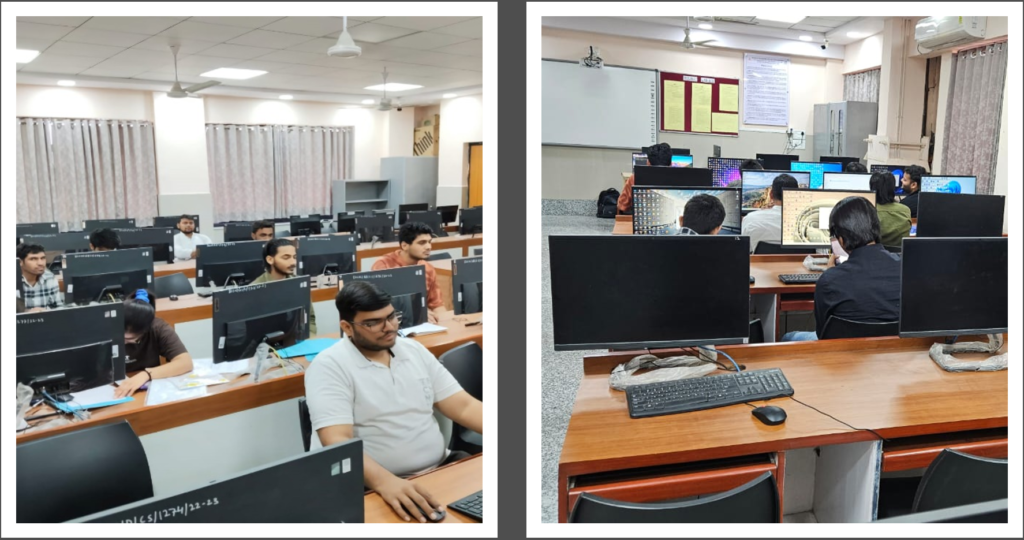 Facilities
Operating System / Software
| Sr. No. |
Name |
Version |
| 1. |
Windows |
10 |
| 2. |
Mentographics Tanner (HEP-1) & (HEP-2) |
|
Hardware
| Sr.No. |
Equipment Name |
Specification |
Quantity |
| 1. |
Computer System |
Intel Core i9 10 Gen 2.10 GH 32 GB RAM |
1 |
| 2. |
Computer System |
Intel Core i5 4 Gen 2.10 GH 16 GB RAM |
2 |
| 3. |
Computer System |
Intel Core i7 8 Gen 3.10 GH 8 GB RAM |
2 |
| 4. |
Computer System |
Intel Core i5 10 Gen 2.10 GH 8 GB RAM |
27 |
| 5. |
Computer System |
GPU System |
1 |
| 6. |
Printer |
HP Laser Jet Pro P1108 |
1 |
Staff
- Lab Incharge: Dr. Annu Dabas
- Lab Assistant: Mr. Depanshu
